(China (Mainland))

Product Summary
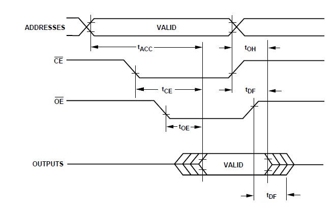
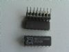
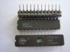
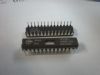
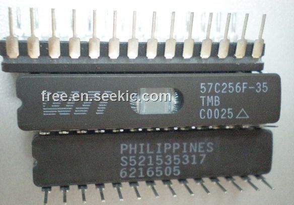
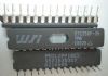
The WS57C256F-35TMB is a High Performance 32K x 8 UV Erasable EPROM. It is manufactured using an advanced CMOS process technology enabling it to operate at speeds as fast as 35 ns Address Access Time (tACC) and 35 ns Chip Enable Time (tCE). The WS57C256F-35TMB was designed utilizing WSI’s patented self-aligned split gate EPROM cell, resulting in a low power device with a very cost effective die size. The low standby power capability of this 256 K product (200μA in a CMOS interface environment) is especially attractive. The WS57C256F-35TMB is available in a variety of package types including the space saving 300 Mil DIP, the surface mount PLDCC, and other windowed and non-windowed options. And its standard JEDEC EPROM pinouts provide for automatic upgrade density paths for current 64K and 128K EPROM users.
Parametrics
WS57C256F-35TMB absolute maximum ratings: (1)Storage Temperature: –65 to + 150℃; (2)Voltage on any Pin with Respect to Ground: -0.6V to +7V; (3)VPP and A9 with Respect to Ground:–0.6V to + 14V; (4)ESD Protection: >2000V.
Features
WS57C256F-35TMB features: (1)Fast Access Time; (2)Immune to Latch-UP: Up to 200mA; (3)Low Power Consumption: 200μA Standby ICC; (4)ESD Protection Exceeds 2000 Volts; (5)Available in 300 Mil DIP and PLDCC; (6)DESC SMD No. 5962-86063.
Diagrams