(China (Mainland))

Product Summary
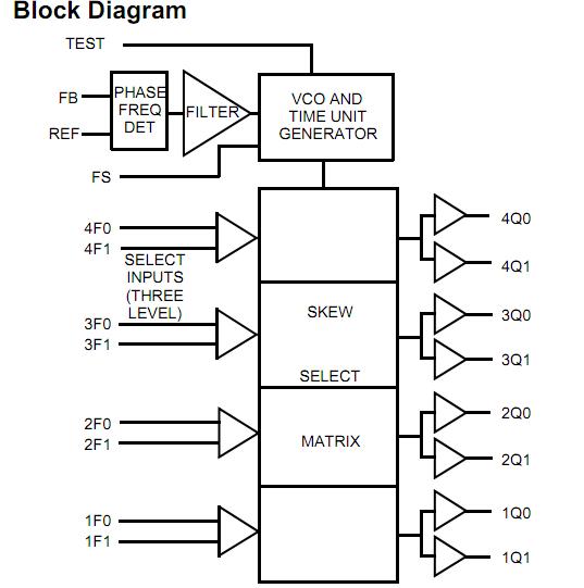
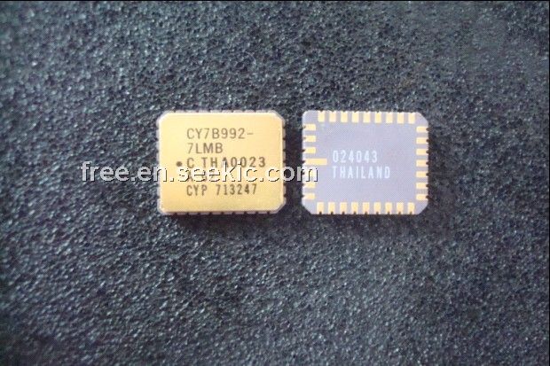
The CY7C992-7LMB is a 200-MHz Low-voltage Programmable Skew Clock Buffer that offers user-selectable control over system clock functions. The CY7C992-7LMB provides the system integrator with functions necessary to optimize the timing of high-performance computer systems. Eight individual drivers, arranged as four pairs of user-controllable outputs, can each drive terminated transmission lines with impedances as low as 50Ω while delivering minimal and specified output skews and full-swing logic levels (LVTTL).
Parametrics
CY7C992-7LMB absolute maximum ratings: (1)VDD, Supply Voltage Nonfunctional: -0.5 to 4.6 VDC; (2)VIN, Input Voltage REF Relative to VCC: -0.5 to 4.6 VDC; (3)VIN, Input Voltage Except REF Relative to VCC: -0.5 to VDD +0.5VDC; (4)LUI, Latch-up Immunity Functional: 300 mA; (5)TS, Temperature, Storage Nonfunctional: -65 to +125℃; (6)TA, Temperature, Operating Ambient Commercial Temperature: 0 to +70℃; (7)TA, Temperature, Operating Ambient Industrial Temperature: -40 +85℃; (8)TJ, Junction Temperature Industrial Temperature: 125℃; (9)θJc, Dissipation, Junction to Case Functional: TBD℃/W; (10)θJa, Dissipation, Junction to Ambient Functional: TBD℃/W; (11)ESDh ESD Protection (Human Body Model): 2000 V.
Features
CY7C992-7LMB features: (1)All output pair skew <100 ps (typical); (2)Input Frequency Range: 3.75 MHz to 200 MHz; (3)Output Frequency Range: 3.75 MHz to 200 MHz; (4)User-selectable output functions, Selectable skew to 18 ns; Inverted and non-inverted; Operation at 1/2 and 1/4 input frequency; Operation at 2x and 4x input frequency (input as low; (5)as 3.75 MHz); (6)Zero input-to-output delay; (7)3.3V Core power supply; (8)Split 2.5V or 3.3V Output power supplies; (9)± 2.5% Output Duty Cycle Distortion for 3.3V Output; (10)LVTTL outputs drive 50Ω terminated lines; (11)Low operating current; (12)32-pin QFN package; (13)Jitter < 100ps peak-to-peak (< 15 ps RMS).
Diagrams